
NEXTECK SINGAPORE PTE LTD
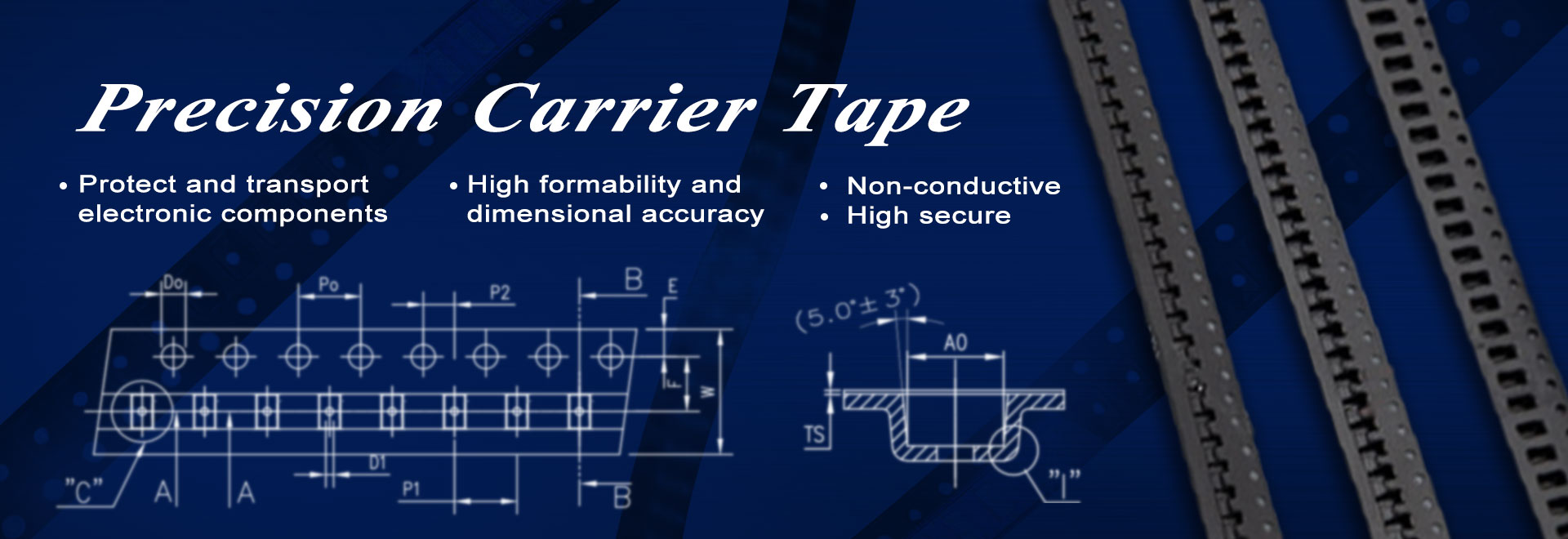
Carrier Tape

ELEGRIP TAPE

COVER TAPE
In semiconductor manufacturing, wafer dicing is a crucial step where processed wafers are cut into individual chips. To p...

AI・Chiplet・Sustainability Ushering a New Era of Semiconductor Manufacturing Though not exhibiting this year, Nexteck ...

At Nexteck, we stay closely tuned to cutting-edge semiconductor advancements. The 70th IEEE IEDM (International Electron ...

Nexteck appreciates your support over the past year...

WASHINGTON—Jan. 17, 2025—The Semiconductor Industry Association (SIA) issued the following statement from SIA Preside...

NEXTECKhasactivelyparticipatedinNEPCONJAPAN,whichhasevolvedalongsidethegrowthoftheelectronicsindustryinJapanandAsia.Theev...

As the holiday season arrives, we would like to express our gratitude for your support this year. Wishing you and your lo...

Looking for enhanced traceability for your products in carrier tape? Nextecks carrier tape comes equipped with high-quali...

Advanced semiconductor packaging combines multiple chips into a single compact unit, offering significant benefits. It in...

© Copyright 2019-2024 NEXTECK. All rights reserved | Design by NEXTECK.COM